


September
12
/ 2021
184
views
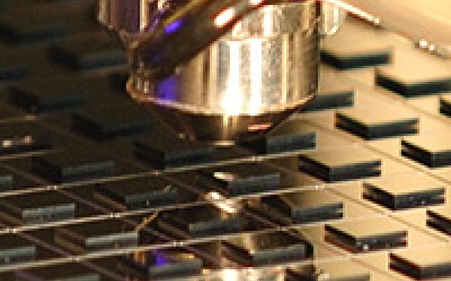
3D packages are emerging in the semiconductor packaging industry to address the serious technical challenges such as miniaturization, faster interconnections, power saving, and limitation to node transition in the front-end process. Typical 3D-package structures are stacked dies with through silicon via (TSV) and micro-bump interconnections, and face-to-face interconnections with micro-bumps for two dies. These are silicon "die" base structure.