
Post categories

  • Home
  • Contact Us
  • Login
  • Register
Home
  • INDUSTRY UPDATES
    • Packaging News
    • Innovations
    • Packaging Offers
    • Press Releases
    • Events
    • resources
  • BLOG
  • OUR PRODUCTS
    • Big Book of Packaging
  • OUR PARTNERS
    • Bernhardt
    • EMA
    • Haemotronic
    • Linhardt
    • Packtoearth
    • Plas-Tech Engineering
    • Roechling
    • Sanok Rubber
    • Schreiner
    • Polycine
    • Yukon Medical
  • SERVICES
    • CONSULTING
    • DESIGN SERVICES

Breadcrumb

  1. Home
  2. 3D Packaging & Wafer-Level Packaging

3D Packaging & Wafer-Level Packaging

Profile picture for user pr011
By pr011 on Mon, 09/13/2021 - 00:01
  • Log in or register to post comments

3D packages are emerging in the semiconductor packaging industry to address the serious technical challenges such as miniaturization, faster interconnections, power saving, and limitation to node transition in the front-end process. Typical 3D-package structures are stacked dies with through silicon via (TSV) and micro-bump interconnections, and face-to-face interconnections with micro-bumps for two dies. These are silicon "die" base structure.

Wafer-level packages (WLP) are the molded die components with redistribution layers, called wafer level CSP (WLCSP). This is a packaged component base structure. Many industry leaders are developing stacked WLCSP just like 3D-package structures to offer inexpensive alternatives to 3D packages.

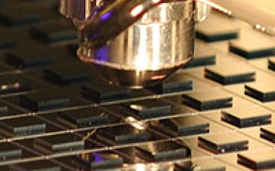
These two packages are often categorized together now. Because of their similar package structures, the challenges are also similar. They need underfill to fill the gaps between stacked dies or molded components. The micro-bumps are too small for mold compounds to fill the gaps, so capillary underfill is the most popular way. For productivity, chip-on­-wafer process is desired: chip-stacking is done multiple times on a wafer, which includes another function as a bottom die. Then these stacked dies are filled with underfill. Tens to hundreds of dies are allocated on the wafer: very tight allocation with hundreds of micron distance to next stacked dies. Dispensing underfill between the stacked dies is thus one of the key challenges because of the narrow distance: small dot size, dispensing position accuracy, and productivity. The productivity means not only faster dispensing but also narrower distance is better for more dies on a wafer.

Key dispensing applications to serve the 3D packaging and WLP industries are:

  • Capillary underfill dispensing for stacked dies and molded components
  • Flux dispensing for die stacking
Image
Source URL
3D Packaging & Wafer-Level Packaging
Tags
3D-package structures
micro-bumps
silicon die base structure

Follow Us

Pro eu apeirian suavitate dissentiet, qui dicunt ancillae id, ne mea homero persequeris.

  • instagram
  • facebook-f
  • twitter

Explore

  • Home
  • Contact Us
  • Login
  • Register

Company

  • Archive
  • Blog
  • Journalists
  • Opinions
First Ever 100% Recyclable Aerosol Spray Cap with Insert, Mono-material: The Sustainable Way to Realize a Fine Spray
27 Jun, 2022
Toblerone chocolate to make a major change from 2023
25 Jun, 2022
Evian launches new recycling reward scheme at Wimbledon
25 Jun, 2022

Footer menu

  • Privacy
  • Terms and conditions
Home
  • INDUSTRY UPDATES
    • Packaging News
    • Innovations
    • Packaging Offers
    • Press Releases
    • Events
    • resources
  • BLOG
  • OUR PRODUCTS
    • Big Book of Packaging
  • OUR PARTNERS
    • Bernhardt
    • EMA
    • Haemotronic
    • Linhardt
    • Packtoearth
    • Plas-Tech Engineering
    • Roechling
    • Sanok Rubber
    • Schreiner
    • Polycine
    • Yukon Medical
  • SERVICES
    • CONSULTING
    • DESIGN SERVICES
Clear keys input element