

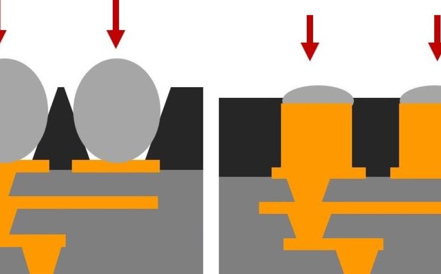

In the world of microelectronics, packaging isn't just about protection — it's about precision, performance, and space optimization. LG Innotek has introduced a breakthrough that may redefine how electronic components are packaged within smartphones and wearables. As smartphone brands push the limits of compact design and battery capacity, LG Innotek has introduced a game-changing solution: replacing traditional solder balls with advanced Copper Post technology to connect chip substrates to motherboards.
Rather than bonding solder balls directly to the substrate surface, LG’s method first places copper columns, followed by soldering on top. This innovative layout allows for 20% tighter spacing between joints without sacrificing electrical performance — enabling thinner devices and more space for features like larger batteries.
But the benefits go beyond space-saving:
- Thermal Advantage: Copper conducts heat 7x more efficiently than traditional solder, helping prevent signal degradation from overheating.
- Higher Density & Performance: Ideal for high-performance interfaces, this structure allows for tighter chip integration.
- Manufacturing Stability: The high melting point of copper prevents deformation during soldering, eliminating the risk of solder balls fusing or misaligning.
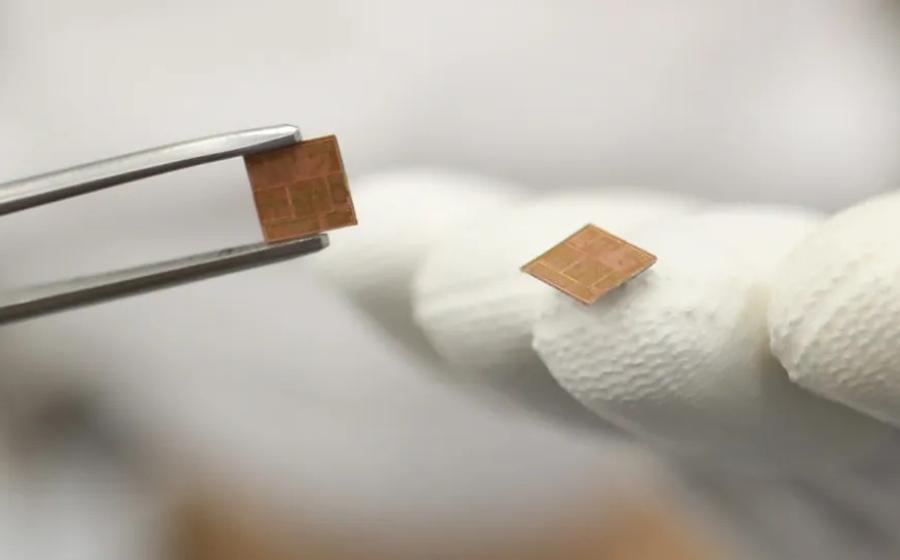
Since 2021, LG Innotek has been developing this tech using 3D digital twin simulations for precision engineering. The company now holds 40+ patents on Copper Post technology and is preparing to deploy it in:
- RF-SiP substrates (modems, amplifiers, filters, etc.)
- FC-CSPs (Flip Chip packages for application processors in smartphones and wearables)
“This innovation isn’t just about components — it’s about helping customers succeed,” said Moon Hyuk-soo, CEO of LG Innotek. “We’re reshaping the substrate industry and delivering differentiated value through cutting-edge packaging solutions.”