plas-tech engineering - Supplier for COC/COP PFS Syringes
Schreiner
rochling

Login Menu

  • Login
  • Register
Home
  • HOME
  • CONNECTIONS
    • Suppliers
    • Buyers
    • Professionals
    • User Companies
    • Softwares
    • Others
  • INDUSTRY UPDATES
    • Packaging News
    • Innovations
    • Press Releases
    • Events
    • Resources
    • Newsletter
    • Testimonials
    • Packaging Interviews
    • Packaging 4 startups
  • BLOG
  • OUR PRODUCTS
    • Big Book of Packaging
  • OUR PARTNERS
    • Bonini
    • Bernhardt
    • EMA
    • Haemotronic
    • Intin
    • Plas-Tech Engineering
    • Polycine
    • Rochling
    • Sanok Rubber
    • Schreiner
    • TARA
    • Yukon Medical
  • SERVICES
    • SUSTAINABLE EXHIBITION
    • CONSULTING
    • DESIGN SERVICES
    • NEWSLETTER SUBSCRIPTION

Breadcrumb

  1. Home
  2. Eco-friendly waterborne semiconductor inks using surfactant

Eco-friendly waterborne semiconductor inks using surfactant

Profile picture for user Madhu Sudan
By Madhu Sudan Si… on Thu, 09/27/2018 - 14:44

Polymer semiconductors are carbon compounds showing the electrical properties of semiconductors. It has been highlighted as a next-generation material of wearable smart devices, etc. not only because they are flexible and light in weight, but also they can be processed in a wide area a low cost through the solution process. However, there is an issue that it causes significant environmental pollution as toxic organic solvents are used in the process.

Despite the limitations, the research team has developed a semiconductor surface control technique using surfactants for environmentally friendly semiconductor manufacturing processes that do not use toxic organic solvents and has produced water-borne semiconductor inks.

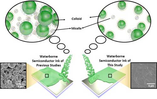
In the study (Energy & Environmental Science, "Universal selection rule for surfactants used in miniemulsion processes for eco-friendly and high performance polymer semiconductors"), the newly developed waterborne semiconductor ink of the research team has small colloidal particles and less surfactant micelles compared to the waterborne semiconductor inks in the previous studies. As a result, it has a relatively flat surface than the conventional waterborne semiconductor inks. The black and white image in the figure shows the comparison of the surface of the thin film made with the waterborne semiconductor ink developed in this study and conventional one.

According to the research team, the technique is expected to be applied in various electronic devices such as P-type and N-type transistors as well as PN diodes, complementary inverters, photodiodes as high-quality thin films.

Professor Chung stressed the significance of the study by stating "This research has fundamentally solved the environmental pollution problem generated during the production of organic semiconductor, which is spotlighted as the core material of wearable electronic devices. We have developed a source technology that can disperse various semiconductor materials into water through the simple chemical modification. We expect that it can be used in various optoelectronic devices ranging from transistors to solar cell, composite circuit, and image sensor.”

https://www.nanowerk.com/nanotechnology-news/newsid=48731.php
  • Log in or register to post comments
plas-tech engineering - Supplier for COC/COP PFS Syringes
YUKON MEDICAL
TARA NIRMAN
schreiner
rochling
3 months ago
Recycling Program Turns Label Waste Into New Packaging
3 months ago
The High-Tech Secrets Behind the Humble Tin Can: A Modern Marvel of Steel Innovation
3 months ago
Recyclability Emerges as Top Priority for European Consumers, Amcor Study Finds

Follow Us

  • linkedin
  • facebook-f
  • twitter

Explore

  • Home
  • Contact Us
  • About us
  • Advertise With Us
  • Login
  • Register
  • Add Testimonial

Company

  • Blog
  • Contact Us
  • Events
  • Packaging News
  • Terms & Conditions
Top 7 Packaging Must-Haves for Personal Care Products
03 May, 2025
FDA
Navigating New FDA Packaging Regulations in 2025: A Complete Guide
29 Apr, 2025
Lamination
Unveiling the Future of Lamination Films: Trends, Challenges & How Purchasers Can Stay Ahead!
26 Apr, 2025

Footer menu

  • Privacy
  • Terms and conditions
  • Contact
Home
  • HOME
  • CONNECTIONS
    • Suppliers
    • Buyers
    • Professionals
    • User Companies
    • Softwares
    • Others
  • INDUSTRY UPDATES
    • Packaging News
    • Innovations
    • Press Releases
    • Events
    • Resources
    • Newsletter
    • Testimonials
    • Packaging Interviews
    • Packaging 4 startups
  • BLOG
  • OUR PRODUCTS
    • Big Book of Packaging
  • OUR PARTNERS
    • Bonini
    • Bernhardt
    • EMA
    • Haemotronic
    • Intin
    • Plas-Tech Engineering
    • Polycine
    • Rochling
    • Sanok Rubber
    • Schreiner
    • TARA
    • Yukon Medical
  • SERVICES
    • SUSTAINABLE EXHIBITION
    • CONSULTING
    • DESIGN SERVICES
    • NEWSLETTER SUBSCRIPTION
Clear keys input element