


Nano-Imprinting and Nano-Assembly
The fields of nano-imprinting and nano-assembly are at the cutting edge of nanotechnology, promising to revolutionize industries from electronics to medicine, including the packaging industry.
Two cutting-edge nanotechnologies—nano-imprinting and nano-assembly—are poised to transform the packaging industry, offering new possibilities for creating smarter, more efficient, and visually appealing packages.
Let's delve into what these processes entail and their potential impact on the future.
Nano-Imprinting: Precision Patterning at the Nanoscale
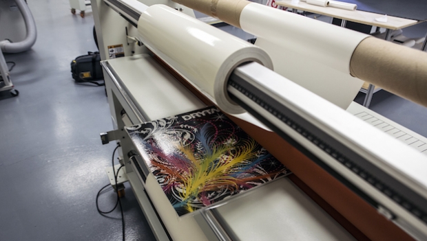
Nano-imprinting lithography (NIL) is a technique used to create nanoscale patterns on a substrate. Unlike traditional photolithography, which relies on light to transfer a pattern, NIL uses a physical mold to imprint the desired pattern onto a surface. It can press intricate patterns with features a thousand times smaller than the width of a human hair.
This method offers several advantages:
High Resolution: NIL can achieve resolutions as fine as a few nanometers, significantly finer than traditional lithographic methods.
Cost-Effectiveness: By bypassing the need for complex light sources and optical systems, NIL can be more economical, especially for high-volume production.
Versatility and Scalability: NIL can be used with a variety of materials, including polymers, metals, and semiconductors, making it suitable for a wide range of applications.
Here's a simplified breakdown of the process:
The Stamp: A mold (stamp) is crafted with the desired nano-pattern. This stamp can be made from various materials like silicon or polymers.
Applying the Pressure: The stamp is pressed onto a material (resist) that can be solidified. Pressure and heat are often used to ensure good contact.
Pattern Transfer: The pattern from the stamp gets imprinted onto the resist after the material solidifies.
Lift-off: The stamp is carefully removed, leaving behind the replicated nanostructure.
Nanoimprinting allows the creation of incredibly precise surface features on packaging materials. Here's how it translates to benefits:
Anti-Counterfeiting Measures: Counterfeiting is a major concern in the packaging of high-value products such as pharmaceuticals, luxury goods, and electronics. NIL can produce intricate, difficult-to-replicate patterns and holograms directly onto packaging materials, enhancing security and authenticity.
Enhanced Aesthetics: NIL allows for the creation of detailed textures and patterns on packaging surfaces, adding a premium look and feel. This can enhance brand perception and make products more appealing on store shelves.
Functional Surfaces: Beyond aesthetics, NIL can be used to impart functional properties to packaging materials. For instance, it can create superhydrophobic surfaces that repel water and other liquids, helping to keep packages clean and dry.
Smart Packaging: Nanoimprinted features can be used to create sensors that detect spoilage or indicate optimal storage conditions.
Sustainability: By enabling precise control over material deposition and patterning, NIL can reduce material waste and enhance the recyclability of packaging. Thinner and more efficient packaging can be achieved without compromising strength or functionality.
Nano-Assembly: Building from the Bottom Up
Nano-assembly refers to the process of organizing nanoparticles into specific structures and configurations. This bottom-up approach contrasts with traditional top-down manufacturing methods, offering greater control over the material's properties and functionalities. There are several key techniques used in nano-assembly:
Self-Assembly: This method relies on the natural tendency of molecules and nanoparticles to arrange themselves into stable, predefined structures without external guidance. Self-assembly can be driven by various forces, including van der Waals forces, electrostatic interactions, and hydrogen bonding.
Directed Assembly: External fields, such as magnetic or electric fields, can be used to guide the assembly of nanoparticles into desired configurations. This method provides more precise control over the final structure compared to self-assembly.
Template-Assisted Assembly: In this technique, pre-patterned templates are used to guide the placement of nanoparticles. This method combines the precision of top-down patterning with the scalability of bottom-up assembly.
Here’s how nano-assembly is being leveraged in the packaging industry:
Biodegradable Materials: Nanoparticles can be used to create bioplastics with improved strength and durability, promoting sustainable packaging options.
Self-healing Packaging: Imagine a package that repairs minor tears or punctures on its own. By incorporating self-assembling molecules, researchers are exploring this possibility for reduced waste.
Smart and Active Packaging: Nanoassembled components can be embedded in packaging to release beneficial gases or absorb unwanted ones, extending shelf life and maintaining product quality.
Future developments may include packaging that actively monitors and interacts with its contents, providing unprecedented levels of protection and information. Additionally, the push towards sustainability will drive the creation of eco-friendly packaging materials that meet both performance and environmental goals.